IsoSol-S100® Polymer-Wrapped Nanotubes
Ultra High-Purity Semiconducting SWNTs
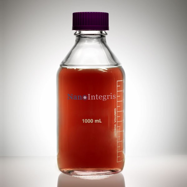
Product Summary
The use of truly scalable and patent-pending technology developed by the National Research Council of Canada, within the Printable Electronics Program, has enabled us to disperse and extract single-walled carbon nanotubes to the highest levels of semiconducting enrichment and purity to date: IsoSol-S100. The starting materials are the purified and highly-scalable RF-plasma grown carbon nanotube supplied by Raymor Nanotech1.
Experimentally, thin film transistors have been prepared from the IsoSol-S100 material on SiO2/Si substrates7, leading to average mobilities exceeding 27cm2/(Vs) and On/Off ratios of 1.8×10⁶. These properties allow the material to be well-suited for ink jet and aerosol jet printing. Haitian Chen from USC says: “Our research group has been able to obtain excellent electrical properties, more specifically mobility of 25 cm2V-1s-1 and current on/off ratio of 4 x 10^6 from thin film transistors (TFTs) based on Nanointegris 99.9% semiconducting carbon nanotube (CNT) solution (IsoSol-S100). It is an outstanding material for the development of CNT-based macroelectronics and flexible macroelectronics. ”
UV-Vis-NIR spectrophotometric assessment of purity2 indicate that this material has semiconducting purities at or greater than 99.9% with the metrics of Itkis Ratio3 and Phi Values4exceeding 0.5 and 0.4, respectively.
The highly graphitized starting material and low sonication intensity utilized for the extraction technique minimizes damage to the nanotubes, allowing the material to exhibit high crysallinity and longer average lengths of 1-2µm, not previously seen when utilizing DGU5 or Chromatography-based6 separation methods.
Additionally, the material is processed in organic solvent with a polymer : nanotube ratio that can be adjusted to less than a factor of four (surfactant : nanotube ratio is 1×10³ in our aqueous surfactant solutions). The solutions also display stabilities of greater than six months. These properties promote great nanotube deposition and adhesion for device creation.
(Click HERE for the official Press Release announcing this product)
1.K. S. Kim, A. Moradian, J. Mostaghimi, Y. Alinejad, A. Shahverdi, B. Simard and G. Soucy, Nano Research, 2009, 2, 800.
2. M. Ouyang , J. Huang , and C.M. Lieber, Acc. Chem. Res. , 2002, 35 (12), 1018-1025.
3. J. Chen, A.M. Rao, S. Lyuksyutov, M.E. Itkis, M.A. Hamon, H. Hu, R.W. Cohn, P.C. Eklund, D.T. Colbert, R.E. Smalley, and R.C. Haddon, J. Phys. Chem. B, 2001, 105 (13), 2525–2528.
4. K.S. Mistry, B.A. Larsen, and J.L. Blackburn, ACS Nano, 2013, 7, 2231-2239.
5. M.S. Arnold, A.A. Green, J.F. Hulvat, S.I. Stupp, and M.C. Hersam, Nat. Nanotechnol., 2008, 3, 387, 394.
6. M. Zheng and E.D. Semke, J. Am. Chem. Soc., 2007, 129, 6084-6085.
7. J. Ding, Z. Li, J. Lefebvre, F. Cheng, G. Dubey, S. Zou, P. Finnie, A. Hrdina, L. Scoles, G.P. Lopinski, C. T. Kingston, B. Simard, and P.R.L. Malenfant, Nanoscale, 2014, 6, 2328-2339.
Product Specifications
| Optical Purity | >99.9% |
| Itkis Ratio (Ї) | >0.5 |
| Phi Value (Φ) | >0.39 |
| Nanotube Concentration | >0.01mg/mL |
| Surfactant : Nanotube Concentration | <4 |
| Standard Solvent Media | Toluene |
| Shelf Life | 3-6 months |
SEM and AFM
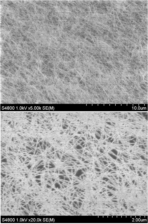
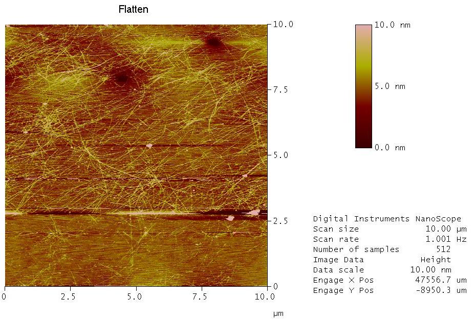
Images used by permission of H. Chen: Nanotechnology Research Laboratory, Department of Electrical Engineering, University of Southern California.
| Diameter Range | 1.2 – 1.4nm |
| Mean Length | 2 µm |
Raman
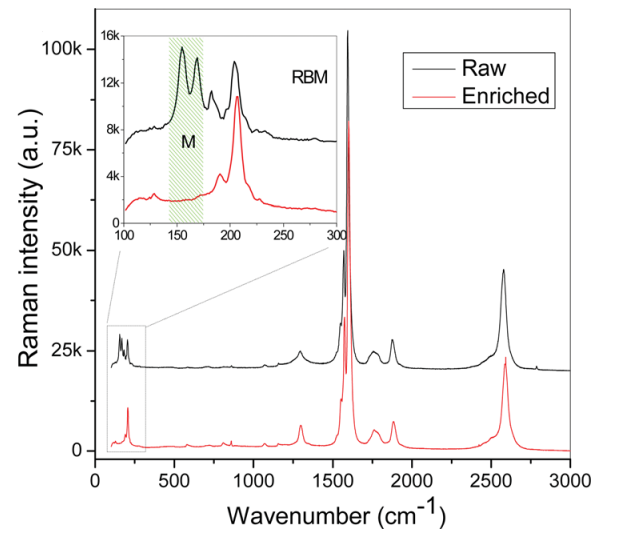
The Radical Breath Mode (RBM) of the spectra excited at 785nm shows that the IsoSol-S100 material has a nearly flat baseline in the metallic region from 145 to 175 cm-1, indicative of a high semiconducting purity.
| Metal Catalyst Impurity | <0.5 % |
| Amorphous Carbon Impurity | <1 % |
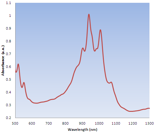
PLE Map
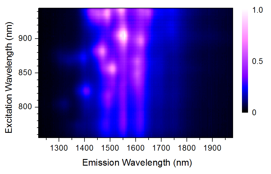
Image used by permission of P. Malenfant: Security and Disruptive Technologies Portfolio, National Research Council Canada.
A photoluminescence excitation (PLE) map for the IsoSol-S100 material shows well resolved (S22, S11) maxima, indicative of well separated nanotubes. UP to 19 (n,m) species contribute to the spectrum, with 8 or 9 having peak intensities higher than or close to 0.5. The (10,9) chirality peak with S11=1570nm and S22=910nm, proved to be the strongest.
Product Applications
The IsoSol-S100 product has been a featured material within numerous research efforts. The primary usage for the IsoSol-S100 material is for the creation of thin film transistors. What makes this material extremely appealing is that its usage enables the creation of thin film transistors that are fully printed, high-performing, flexible, stable, scalable, and low cost, with the capacity to span large areas.
Active Matrix Electrochromic Displays
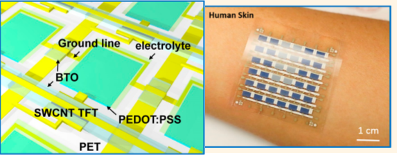
At the University of Southern California, an active-matrix electrochromic display was created utilizing NanoIntegris’ IsoSol-S100 material. [1] The SWCNT thin film transistors had channel lengths of ~105 um and channel widths of ~1000 µm. The TFT exhibited an on-state current density of 3.62 µA/mm at source drain voltage (VDS)= -1V and gate voltage (VG) = -15V with an average on-off ratio of 104. The average mobility was ~3.92 cm2/Vs. These results from the fully screen-printed TFT array were comparable wth Javey and Cho’s work on gravure printed CNT TFT’s [2] and backplanes [3,4] and showed the potential to enable new applications such as monolithically integrated active-matrix organic light-emitting diodes (AMOLED) and backplanes desirable for practical applications such as large-area active matrix-based flexible displays and sensing systems.
[1] ACS Nano 2016, 10, 9816-9822.
[2] Nano Lett. 2013, 13, 3864-9.
[3] Adv. Mater. 2015, 27, 1561.
[4] Adv. Mater. 2002, 14, 1460
Fully Printed Thin Film Transistors [1]
NanoIntegris’ IsoSol-S100 material was ink-jet printed at 93 mg/L onto silicon test chips using <20µm drop spacing. The transistors had dense uniform network spanning the source and drain with an average hole mobilities of ~30 cm2/Vs, and on-state current densities greater than 0.75 mA/mm, with on/off ratios of 106.
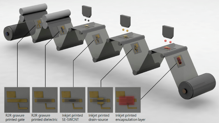
Transistors were generated on flexible polyethylene terephthalate (PET) substrate with silver gate electrodes and high-k BaTiO3 dilelectric layers, printed via a R2R gravure printing process. The IsoSol-S100 was inkjet printed at 50 mg/L along with silver source/ drain contacts, defining a channel of 1000 µm x 150 µm. The on/off ratios were determined to be 7×10⁴ with a subthreshold swing of 1.8V/decade, a transconductance of 0.26 µS/V, a threshold voltage of -2.5V, a calculated capacitance of 6.5 nF/cm2, and a mobility of 6cm2/Vs.
[1] ACS Appl. Mater. Interfaces 2016, 8, 27900-27910.
Product Delivery
We currently offer this nanotube product in two forms:
1. Aromatic-based (toluene, xylenes, etc.) polymer solution at 0.01 – 0.3 mg CNTs / mL or above.
2. Solvent-free thin film with polymer wrapping (Polymer:CNT ratio is typically 4 or below).
NOTE: We remove the solvent from our solutions via a proprietary process that involves filtration and rinsing. The end result is a film-like structure, otherwise known as a bucky paper. Our thin films have been formulated so that they are easy to use, break apart, and disperse in solvents, using gentle sonication.
Prices
Gram and multi-gram price quotes available by request. Additional discounts also available for large volume orders.
To place and order contact our Sales Manager at sales@nanointegris.com or call +1-866-650-0482.
| Form | Price (USD) |
|---|---|
| Solution | $850 |
| Thick Film | $950 |